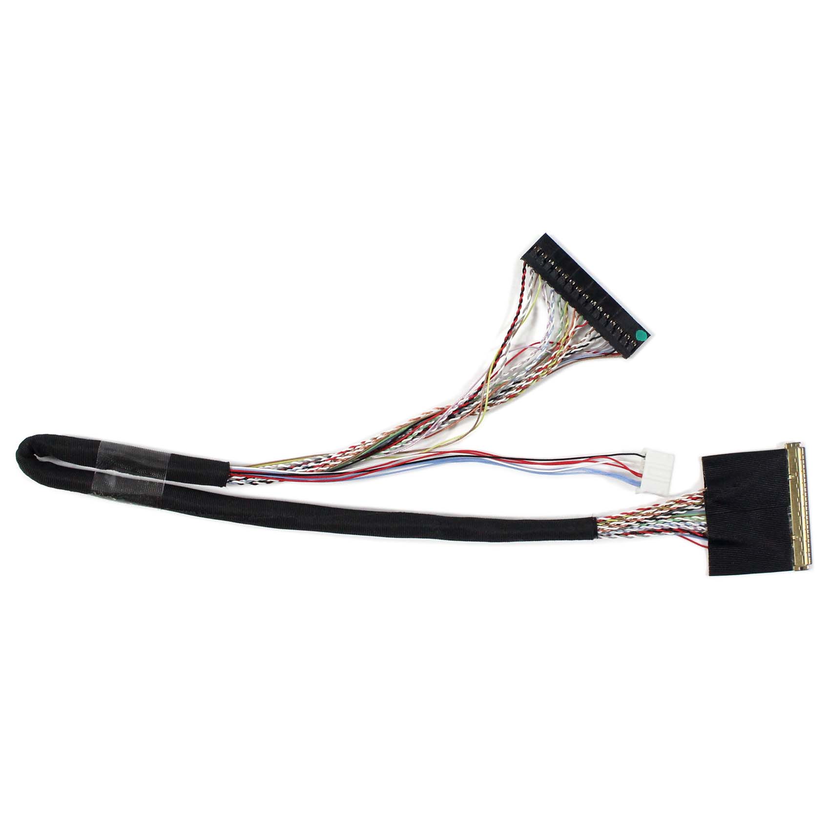
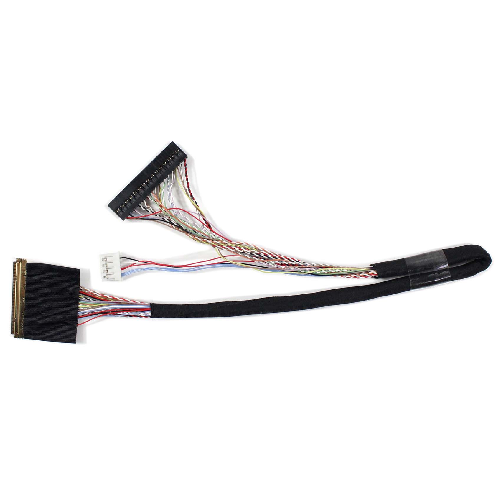
Connection the LCD Controller Board:
PIN # | SIGNAL NAME | DESCRIPTION |
1 | VSEL | Power for panel |
2 | VSEL | Power for panel |
3 | VSEL | Power for panel |
4 | GND | Ground |
5 | GND | Ground |
6 | GND | Ground |
7 | RXO0- | Negative LVDS differential data input |
8 | RXO0+ | Positive LVDS differential data input |
9 | RXO1- | Negative LVDS differential data input |
10 | RXO1+ | Positive LVDS differential data input |
11 | RXO2- | Negative LVDS differential data input |
12 | RXO2+ | Positive LVDS differential data input |
13 | GND | Ground |
14 | GND | Ground |
15 | RXOC- | Negative LVDS differential clock input |
16 | RXOC+ | Positive LVDS differential clock input |
17 | RXO3- | No Connection |
18 | RXO3+ | No Connection |
19 | RXE0- | LVDS EVEN 0 - Signal |
20 | RXE0+ | LVDS EVEN 0 + Signal |
21 | RXE1- | LVDS EVEN 1 - Signal |
22 | RXE1+ | LVDS EVEN 1 + Signal |
23 | RXE2- | LVDS EVEN 2 - Signal |
24 | RXE2+ | LVDS EVEN 2 + Signal |
25 | GND | Ground |
26 | GND | Ground |
27 | RXEC- | LVDS EVEN Clock - Signal |
28 | RXEC+ | LVDS EVEN Clock + Signal |
29 | RXE3- | LVDS EVEN 3 - Signal |
30 | RXE3+ | LVDS EVEN 3 + Signal |
Connection the LCD Screen
1 | NC | No connection |
2 | VDD | Power Supply +3.3V |
3 | VDD | Power Supply +3.3V |
4 | VDDEDID | EDID +3.3V Power |
5 | NC | No connection |
6 | CLK_EDID | EDID Clock Input |
7 | DATA_EDID | EDID Data Input |
8 | GND | Ground |
9 | RXOIN0N | Negative LVDS Differential Data INPUT for odd pixel |
10 | RXOIN0P | Positive LVDS Differential Data INPUT for odd pixel |
11 | GND | Ground |
12 | RXOIN1N | Negative LVDS Differential Data INPUT for odd pixel |
13 | RXOIN1P | Positive LVDS Differential Data INPUT for odd pixel |
14 | GND | Ground |
15 | RXOIN2N | Negative LVDS Differential Data INPUT for odd pixel |
16 | RXOIN2P | Positive LVDS Differential Data INPUT for odd pixel |
17 | GND | Ground |
18 | RXOCLKINN | Negative LVDS Differential Clock INPUT for odd pixel |
19 | RXOCLKINP | Positive LVDS Differential Clock INPUT for odd pixel |
20 | GND | Ground |
21 | RXOIN3N | Negative LVDS Differential Data INPUT for odd pixel |
22 | RXOIN3P | Positive LVDS Differential Data INPUT for odd pixel |
23 | GND | Ground |
24 | RXEIN0N | Negative LVDS Differential Data INPUT for even pixel |
25 | RXEIN0P | Positive LVDS Differential Data INPUT for even pixel |
26 | GND | Ground |
27 | RXEIN1N | Negative LVDS Differential Data INPUT for even pixel |
28 | RXEIN1P | Positive LVDS Differential Data INPUT for even pixel |
29 | GND | Ground |
30 | RXEIN2N | Negative LVDS Differential Data INPUT for even pixel |
31 | RXEIN2P | Positive LVDS Differential Data INPUT for even pixel |
32 | GND | Ground |
33 | RXECLKINN | Negative LVDS Differential Clock INPUT for even pixel |
34 | RXECLKINN | Positive LVDS Differential Clock INPUT for even pixel |
35 | GND | Ground |
36 | RXEIN3N | Negative LVDS Differential Data INPUT for even pixel |
37 | RXEIN3P | Positive LVDS Differential Data INPUT for even pixel |
38 | GND | Ground |
39 | DCR_EN (CABC_EN) | Dynamic backlight control |
40 | PWM_IN | System PWM signal input for dimming |
41 | PWM_OUT | Panel PWM signal output to system |
42 | NC | No connection |
43 | LED_CA5 | LED Cathode 5 |
44 | LED_CA4 | LED Cathode 4 |
45 | LED_CA3 | LED Cathode 3 |
46 | LED_CA2 | LED Cathode 2 |
47 | LED_CA1 | LED Cathode 1 |
48 | NC | No connection |
49 | VLED Output | LED Backlight power |
50 | VLED Output | LED Backlight power |
Packing list :
1×IPEX 50P 2ch 8bit LVDS cable 300mm for B101UAN01 B10UAN02 B101UAT02